
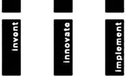
USPTO serial 79131711
INVENT INNOVATE IMPLEMENT
Reviewed by CopyMark Law Group
- Filing date
- Status date
- Registration date
- May 27, 2014
- Examiner
- SHANOSKI, JOANNA MARIE
- Law office
- Historical data usage
What this means
This trademark is registered with the USPTO. Monitoring new filings can help you catch lookalike marks early.
Need help with INVENT INNOVATE IMPLEMENT?
If you own this trademark, we can monitor new filings and help with USPTO deadlines. If you do not, we can file a new U.S. application.
Owner
IBG Immobilien und Beteiligungs GmbH
AT
Other trademarks owned by IBG Immobilien und Beteiligungs GmbH
IBG Immobilien und Beteiligungs; GmbH
AT
Other trademarks owned by IBG Immobilien und Beteiligungs; GmbH
IBG Immobilien und Beteiligungs; GmbH
AT
Other trademarks owned by IBG Immobilien und Beteiligungs; GmbH
Attorney of record
The USPTO lists this attorney as the applicant's representative for correspondence on this application.
Stacy L. Emhoff
Stacy L. Emhoff Walker & Jocke Co., LPA231 South BroadwayMedina, OH 44256United StatesGoods and services
| Class | Description | Status | First use |
|---|---|---|---|
| 007 | Machines and apparatus for producing, aligning, adjusting, bonding, coating, laminating, developing, cleaning, printing, irradiating, thermal treatment and lithographic treatment, namely, nanostructure-imprinting machines, hot embossing machines, micro-contact printing machines, and packaging machines for electronic circuitry or semi-conductors; parts and equipment, namely, fittings, bearings, chucks, joints and lubricating apparatus for the aforesaid machines and apparatus, included in this class | ACTIVE | — |
| 009 | Computer software for use in processing equipment for processing of electronic circuitry or semi-conductors, in particular of transistors or wafers; machines and apparatus for testing, namely, testing machines for semiconductors, tensile testing machines, optical inspection apparatus for inspection of semiconductor materials; Electronic apparatus for testing semiconductor wafer conductivity and circuitry testing; ultrasonic inspection devices for non-medical and non-destructive testing, metal strength testing machines, semi-conductor wafer probes and wafer test metrology equipment for nanostructure-imprinting, hot-embossing, micro-contact printing, wafer testing, and package testing machines for electronic circuitry or semi-conductors; parts and equipment for the aforesaid machines and apparatus, included in this class, namely, batteries, electric wires and cables | ACTIVE | — |
| 042 | Technical consultancy, for others, in relation to methods and devices in the field of semiconductor technology, namely, research and design in the area of semiconductor systems, semiconductor cell libraries, wafers and integrated circuits, semiconductor packages, semiconductor testing devices, semiconductor handling and storage devices and semiconductor processing technology; contractual research and contractual development, for others, in relation to methods and devices in the field of semiconductor technology; technical system engineering, for others, in relation to methods and devices in the field of semiconductor technology | ACTIVE | — |
Related trademarks
CopyMark links this record to cited §2(d) serials, the owner's other marks, Nice classes, similar mark names, and recently changed USPTO applications.
- Other trademarks owned by IBG Immobilien und Beteiligungs GmbH
- Other trademarks owned by IBG Immobilien und Beteiligungs; GmbH
- Other trademarks owned by IBG Immobilien und Beteiligungs; GmbH
- Other trademarks in Class 007
- Other trademarks in Class 009
- Other trademarks in Class 042
- Similar marks named INVENT INNOVATE IMPLEMENT
- Recently changed USPTO trademarks
- Recently filed trademarks
- Browse all trademark records
Prosecution history
| Date | Code | Event | What it means |
|---|---|---|---|
| Nov 20, 2024 | NA71 | NOTICE OF ACCEPTANCE OF SEC. 71 - E-MAILED | — |
| Nov 20, 2024 | 71AG | REGISTERED-SEC.71 ACCEPTED | — |
| Nov 18, 2024 | APRE | CASE ASSIGNED TO POST REGISTRATION PARALEGAL | — |
| Apr 4, 2024 | ES71 | TEAS SECTION 71 RECEIVED | — |
| May 27, 2023 | REM4 | COURTESY REMINDER - SEC. 71 (10-YR) E-MAILED | — |
| Dec 31, 2022 | RNWL | INTERNATIONAL REGISTRATION RENEWED | — |
| Aug 31, 2020 | NA75 | NOTICE OF ACCEPTANCE OF SEC. 71 & 15 - E-MAILED | — |
| Aug 31, 2020 | C75A | REGISTERED - SEC. 71 ACCEPTED & SEC. 15 ACK. | — |
| Jul 21, 2020 | APRE | CASE ASSIGNED TO POST REGISTRATION PARALEGAL | — |
| Jun 11, 2020 | NREP | NEW REPRESENTATIVE AT IB RECEIVED | — |
| May 19, 2020 | ES75 | TEAS SECTION 71 & 15 RECEIVED | — |
| May 27, 2019 | REM3 | COURTESY REMINDER - SEC. 71 (6-YR) E-MAILED | — |
| Nov 8, 2014 | FINO | FINAL DECISION TRANSACTION PROCESSED BY IB | — |
| Oct 17, 2014 | FICS | FINAL DISPOSITION NOTICE SENT TO IB | — |
| Oct 17, 2014 | FIMP | FINAL DISPOSITION PROCESSED | — |
| Aug 27, 2014 | FICR | FINAL DISPOSITION NOTICE CREATED, TO BE SENT TO IB | — |
| May 27, 2014 | R.PR | REGISTERED-PRINCIPAL REGISTER | Your trademark is registered on the Principal Register — the strongest form of federal trademark protection. You may use the ® symbol for the covered goods and services. Maintenance filings (Section 8 and renewals) are required to keep the registration alive. |
| Mar 11, 2014 | NPUB | OFFICIAL GAZETTE PUBLICATION CONFIRMATION E-MAILED | — |
| Mar 11, 2014 | PUBO | PUBLISHED FOR OPPOSITION | Your mark was published in the USPTO Official Gazette for a 30-day opposition window. During that period, third parties who believe they would be harmed can file an opposition. If no opposition is filed, prosecution usually continues toward registration or a Notice of Allowance. |
| Mar 7, 2014 | GPNX | NOTIFICATION PROCESSED BY IB | — |
| Feb 19, 2014 | OPNS | NOTIFICATION OF POSSIBLE OPPOSITION SENT TO IB | — |
| Feb 19, 2014 | OP2R | NOTICE OF START OF OPPOSITION PERIOD CREATED, TO BE SENT TO IB | — |
| Feb 19, 2014 | NONP | NOTIFICATION OF NOTICE OF PUBLICATION E-MAILED | — |
| Jan 31, 2014 | PREV | LAW OFFICE PUBLICATION REVIEW COMPLETED | — |
| Jan 31, 2014 | ALIE | ASSIGNED TO LIE | — |
| Jan 10, 2014 | CNSA | APPROVED FOR PUB - PRINCIPAL REGISTER | — |
| Jan 9, 2014 | TEME | TEAS/EMAIL CORRESPONDENCE ENTERED | — |
| Jan 9, 2014 | CRFA | CORRESPONDENCE RECEIVED IN LAW OFFICE | — |
| Jan 9, 2014 | TROA | TEAS RESPONSE TO OFFICE ACTION RECEIVED | This event means the applicant filed a response to a USPTO Office Action — typically arguments, amendments, or evidence addressing the examiner's objections. The USPTO will review the response and either allow the mark to proceed or issue another action. |
| Dec 27, 2013 | GNRN | NOTIFICATION OF NON-FINAL ACTION E-MAILED | A non-final Office Action means the USPTO examining attorney has raised at least one issue with your trademark application but has not made a final decision. You usually have three months to respond with arguments, amendments, or evidence. Missing the deadline can abandon the application. |
| Dec 27, 2013 | GNRT | NON-FINAL ACTION E-MAILED | A non-final Office Action means the USPTO examining attorney has raised at least one issue with your trademark application but has not made a final decision. You usually have three months to respond with arguments, amendments, or evidence. Missing the deadline can abandon the application. |
| Dec 27, 2013 | CNRT | NON-FINAL ACTION WRITTEN | A non-final Office Action means the USPTO examining attorney has raised at least one issue with your trademark application but has not made a final decision. You usually have three months to respond with arguments, amendments, or evidence. Missing the deadline can abandon the application. |
| Dec 20, 2013 | TEME | TEAS/EMAIL CORRESPONDENCE ENTERED | — |
| Dec 20, 2013 | CRFA | CORRESPONDENCE RECEIVED IN LAW OFFICE | — |
| Dec 20, 2013 | TROA | TEAS RESPONSE TO OFFICE ACTION RECEIVED | This event means the applicant filed a response to a USPTO Office Action — typically arguments, amendments, or evidence addressing the examiner's objections. The USPTO will review the response and either allow the mark to proceed or issue another action. |
| Aug 4, 2013 | RFNT | REFUSAL PROCESSED BY IB | — |
| Jul 15, 2013 | RFCS | NON-FINAL ACTION MAILED - REFUSAL SENT TO IB | — |
| Jul 15, 2013 | RFRR | REFUSAL PROCESSED BY MPU | — |
| Jul 13, 2013 | MAFR | APPLICATION FILING RECEIPT MAILED | — |
| Jul 12, 2013 | RFCR | NON-FINAL ACTION (IB REFUSAL) PREPARED FOR REVIEW | — |
| Jul 11, 2013 | CNRT | NON-FINAL ACTION WRITTEN | A non-final Office Action means the USPTO examining attorney has raised at least one issue with your trademark application but has not made a final decision. You usually have three months to respond with arguments, amendments, or evidence. Missing the deadline can abandon the application. |
| Jul 9, 2013 | DOCK | ASSIGNED TO EXAMINER | — |
| Jul 9, 2013 | NWOS | NEW APPLICATION OFFICE SUPPLIED DATA ENTERED | — |
| Jul 5, 2013 | LIMI | LIMITATION FROM ORIGINAL APPLICATION ENTERED | — |
| Jul 4, 2013 | REPR | SN ASSIGNED FOR SECT 66A APPL FROM IB | — |