
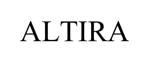
USPTO serial 98632652
ALTIRA
Reviewed by CopyMark Law Group
Status 606
- Filing date
- Status date
- Registration date
- —
- Examiner
- MAI, TINA HSIN
- Law office
- INTENT TO USE SECTION
What this means
This page summarizes the public USPTO record for this serial number, including owners, goods and services, and prosecution history.
Need help with ALTIRA?
If you own this trademark, we can monitor new filings and help with USPTO deadlines. If you do not, we can file a new U.S. application.
Current trademark owner
Monitor this mark, or talk with CopyMark about this registration.
Not the owner?
File a new U.S. trademark application, or speak with our attorneys.
Owner
Attorney of record
The USPTO lists this attorney as the applicant's representative for correspondence on this application.
Cynthia L. Pillote
Cynthia L. Pillote Snell & Wilmer L.L.P.1 East Washington St., Suite 2700Phoenix, AZ 85004United StatesGoods and services
| Class | Description | Status | First use |
|---|---|---|---|
| 007 | Machines and machine tools for the assembly and packaging of electronic chips and structural parts and fittings therefor; machines for manufacturing semiconductors, and structural parts and fittings therefor; semiconductor manufacturing machines; semiconductor manufacturing machines and systems composed of a vacuum chamber for accommodating semiconductor wafers and structural parts and fittings therefor; structural parts and machines for handling and transferring semiconductor wafers into and out of vacuum chambers, and structural parts and fittings therefor; machines and machine tools for the treatment of semiconductor wafers, namely, thermal treatment reactors and chemical vapor deposition reactors, chemical reactors for the thermal treatment of semiconductor wafers; machines for the plasma assisted manufacture of semiconductors, namely, vacuum treatment machines for plasma assisted deposition, and vacuum machines for depositing fine films; plasma enhanced deposition machines, namely, semiconductor manufacturing machines utilizing plasma-enhanced deposition, and structural parts and fittings therefor; industrial surface treatment equipment, namely, vacuum plasma treatment systems comprised of a high frequency, high voltage generator, controls, and treatment chamber, and structural fittings and parts therefor; semiconductor wafer processing reactors for the chemical treatment and the thermal treatment of semiconductor wafers and for the chemical cleaning of semiconductor wafers by means of a gas phase process, also with the use of plasma, namely, gas discharge industrial chemical reactors, and structural parts and fittings therefor; industrial robots for the handling of semiconductor wafers; industrial gas-phase reactors for processing semiconductor wafers, namely, chemical reactors for the thermal treatment of semiconductor wafers and reactors for chemical vapor deposition for depositing thin films on semiconductor wafers; industrial gas-phase semiconductor wafer processing reactors for the chemical treatment and the thermal treatment of semiconductor wafers and for the chemical cleaning of semiconductor wafers by means of a gas phase process, also with the use of gas discharge; and structural and replacement parts for the aforementioned products | ACTIVE | — |
| 009 | Electrical reactors for processing semiconductor wafers; laboratory gas-phase reactors for processing semiconductor wafers, namely, chemical reactors for the thermal treatment of semiconductor wafers and reactors for chemical vapor deposition for depositing thin films on semiconductor wafers; laboratory chemical reactors; laboratory gas-phase semiconductor wafer processing reactors for the chemical treatment and the thermal treatment of semiconductor wafers and for the chemical cleaning of semiconductor wafers by means of a gas phase process, also with the use of gas discharge; and structural and replacement parts for the aforementioned products; robots being electronic control devices, namely, laboratory robots; electronic controllers for industrial robots for use by the semiconductor industry; electronic controllers for controlling semiconductor wafer processing machines; electronic control systems for semiconductor manufacturing machines; structural parts and fittings for the aforementioned goods | ACTIVE | — |
Related trademarks
CopyMark links this record to cited §2(d) serials, the owner's other marks, Nice classes, similar mark names, and recently changed USPTO applications.
Prosecution history
| Date | Code | Event | What it means |
|---|---|---|---|
| Apr 6, 2026 | MAB6 | ABANDONMENT NOTICE E-MAILED - NO USE STATEMENT FILED | The intent-to-use application was abandoned because no acceptable Statement of Use (or valid extension) was filed before the Notice of Allowance deadline expired. The application is dead unless revived within a limited window. |
| Apr 6, 2026 | ABN6 | ABANDONMENT - NO USE STATEMENT FILED | The intent-to-use application was abandoned because no acceptable Statement of Use (or valid extension) was filed before the Notice of Allowance deadline expired. The application is dead unless revived within a limited window. |
| Sep 2, 2025 | NOAM | NOA E-MAILED - SOU REQUIRED FROM APPLICANT | A Notice of Allowance means your intent-to-use application cleared examination and opposition but is not registered yet. You must file a Statement of Use showing the mark in commerce, or request an extension, before the deadline — usually six months from the notice date. |
| Jul 8, 2025 | NPUB | OFFICIAL GAZETTE PUBLICATION CONFIRMATION E-MAILED | — |
| Jul 8, 2025 | PUBO | PUBLISHED FOR OPPOSITION | Your mark was published in the USPTO Official Gazette for a 30-day opposition window. During that period, third parties who believe they would be harmed can file an opposition. If no opposition is filed, prosecution usually continues toward registration or a Notice of Allowance. |
| Jul 2, 2025 | NONP | NOTIFICATION OF NOTICE OF PUBLICATION E-MAILED | — |
| Jun 2, 2025 | CNSA | APPROVED FOR PUB - PRINCIPAL REGISTER | — |
| Jun 2, 2025 | XAEC | EXAMINER'S AMENDMENT ENTERED | — |
| Jun 2, 2025 | GNEN | NOTIFICATION OF EXAMINERS AMENDMENT E-MAILED | — |
| Jun 2, 2025 | GNEA | EXAMINERS AMENDMENT E-MAILED | — |
| Jun 2, 2025 | CNEA | EXAMINERS AMENDMENT -WRITTEN | — |
| Apr 28, 2025 | EWAF | TEAS WITHDRAWAL OF ATTORNEY RECEIVED-FIRM RETAINS | — |
| Apr 28, 2025 | TCCA | TEAS CHANGE OF CORRESPONDENCE RECEIVED | — |
| Apr 28, 2025 | ARAA | ATTORNEY/DOM.REP.REVOKED AND/OR APPOINTED | This event means the applicant filed a response to a USPTO Office Action — typically arguments, amendments, or evidence addressing the examiner's objections. The USPTO will review the response and either allow the mark to proceed or issue another action. |
| Apr 28, 2025 | REAP | TEAS REVOKE/APP/CHANGE ADDR OF ATTY/DOM REP RECEIVED | — |
| Apr 28, 2025 | TEME | TEAS/EMAIL CORRESPONDENCE ENTERED | — |
| Apr 28, 2025 | CRFA | CORRESPONDENCE RECEIVED IN LAW OFFICE | — |
| Apr 28, 2025 | TROA | TEAS RESPONSE TO OFFICE ACTION RECEIVED | This event means the applicant filed a response to a USPTO Office Action — typically arguments, amendments, or evidence addressing the examiner's objections. The USPTO will review the response and either allow the mark to proceed or issue another action. |
| Jan 28, 2025 | GNRN | NOTIFICATION OF NON-FINAL ACTION E-MAILED | A non-final Office Action means the USPTO examining attorney has raised at least one issue with your trademark application but has not made a final decision. You usually have three months to respond with arguments, amendments, or evidence. Missing the deadline can abandon the application. |
| Jan 28, 2025 | GNRT | NON-FINAL ACTION E-MAILED | A non-final Office Action means the USPTO examining attorney has raised at least one issue with your trademark application but has not made a final decision. You usually have three months to respond with arguments, amendments, or evidence. Missing the deadline can abandon the application. |
| Jan 28, 2025 | CNRT | NON-FINAL ACTION WRITTEN | A non-final Office Action means the USPTO examining attorney has raised at least one issue with your trademark application but has not made a final decision. You usually have three months to respond with arguments, amendments, or evidence. Missing the deadline can abandon the application. |
| Jan 22, 2025 | DOCK | ASSIGNED TO EXAMINER | — |
| Jan 14, 2025 | NWOS | NEW APPLICATION OFFICE SUPPLIED DATA ENTERED | — |
| Jul 3, 2024 | NWAP | NEW APPLICATION ENTERED | — |