
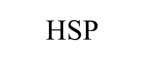
USPTO serial 99517294
HSP
Reviewed by CopyMark Law Group
Status 688Notice of Allowance
- Filing date
- Status date
- Registration date
- —
- Examiner
- STEINPFAD, SARAH E
- Law office
- INTENT TO USE SECTION
What this means
The USPTO has issued a Notice of Allowance. To complete registration you generally need to file a Statement of Use or an extension request before the deadline.
Need help with HSP?
If you own this trademark, we can monitor new filings and help with USPTO deadlines. If you do not, we can file a new U.S. application.
Current trademark owner
Get help with this Notice of Allowance, set up monitoring, or talk with CopyMark.
Get Attorney Assistance for just $947*
Plus Government fees of $450
Not the owner?
File a new U.S. trademark application, or speak with our attorneys.
Owner
Hiki-gun, Saitama, JP
Hiki-gun, Saitama, JP
Attorney of record
The USPTO lists this attorney as the applicant's representative for correspondence on this application.
Kumiko Ide
Kumiko Ide WENDEROTH, LIND & PONACK, LLP1025 Connecticut Avenue NW, Suite 500Washington, DC 20036United StatesGoods and services
| Class | Description | Status | First use |
|---|---|---|---|
| 001 | Chemicals for use in the process of producing printed circuit boards, namely, resist ink in the nature of solder mask; chemicals for use in the process of producing printed circuit boards, namely, resist ink in the nature of photoresists; chemicals for use in the process of producing printed circuit boards, namely, solder resists; chemical preparations for use in the process of producing printed circuit boards, namely, solder mask; etching resist; photoresists; chemical preparations for use in photography; photosensitive resists in the nature of solder mask in the form of film for use in the process of producing printed circuit boards; photosensitive resists in the nature of photoresists in the form of film for use in the process of producing printed circuit boards; dry films for electronic components; photosensitive resists in the form of film for sealing electronic components; insulation dry films for electronic components; thermal curing type dry films for electronic components; chemical preparations for blocking light; chemical coatings for use in the process of producing printed circuit boards; heat resisting materials, namely, heat resisting unprocessed artificial resin for electronic components; chemical preparations for industrial purposes; industrial chemicals; glue and adhesives for industrial purposes; chemical preparations, namely, thermal interface materials for electronic components for use as a filler to enhance the thermal conductivity between components | ACTIVE | — |
| 002 | Dyes for general industrial use; pigments; paints for blocking light; marking inks in the nature of printing inks for use in the process of producing printed circuit boards; marking inks for use in the process of producing electronic components; inks for hole plugging, namely, printing inks for use in the process of producing printed circuit boards; paints for sealing electronic components; heat-resistant paints; paints; printing inks for use in the process of producing printed circuit boards; printing inks for use in the process of producing electronic components; printing ink | ACTIVE | — |
| 017 | Electrical insulating resists, namely, electrical insulating materials in the liquid form for use in the process of producing printed circuit boards; insulating resin materials for use in the process of producing printed circuit boards; insulating resin materials for use in the process of producing electronic components; insulating resin materials for interlayer dielectric materials in the liquid form for use in the process of producing build-up boards; insulating resin materials for interlayer dielectric materials in the liquid form for sealing electronic components; insulating resin materials for interlayer dielectric materials for use in the process of producing build-up boards; insulating resin materials for interlayer dielectric materials for sealing electronic components; insulating resin materials for interlayer dielectric materials in the form of dry film for use in the process of producing build-up boards; insulating resin materials for interlayer dielectric materials in the form of dry film for sealing electronic components; insulating coating materials for use in the process of producing printed circuit boards; insulating coating materials for use in the process of producing display panels; insulating coating materials for protecting copper foil on the surface of printed circuit boards; insulating coating materials for use in the process of producing package application boards; insulating coating materials for use in the process of producing flexible printed circuit boards; insulating fillers, namely, insulating materials for protecting copper foil used with holes of printed circuit boards; insulating materials for sealing electronic components; insulating resin materials for sealing electronic components; electrical insulating materials for use in the process of producing printed circuit boards; semi-processed plastics; thermally conductive insulating resin materials for electronic components; insulating materials; electrical insulating materials | ACTIVE | — |
Related trademarks
CopyMark links this record to cited §2(d) serials, the owner's other marks, Nice classes, similar mark names, and recently changed USPTO applications.
- Other trademarks owned by TAIYO HOLDINGS CO., LTD.
- Other trademarks owned by TAIYO HOLDINGS CO., LTD.
- Other trademarks in Class 001
- Other trademarks in Class 002
- Other trademarks in Class 017
- Similar marks named HSP
- Prosecution event NOAM explained
- Recently changed USPTO trademarks
- Recently filed trademarks
- Browse all trademark records
Prosecution history
| Date | Code | Event | What it means |
|---|---|---|---|
| Jul 7, 2026 | NOAM | NOA E-MAILED - SOU REQUIRED FROM APPLICANT | A Notice of Allowance means your intent-to-use application cleared examination and opposition but is not registered yet. You must file a Statement of Use showing the mark in commerce, or request an extension, before the deadline — usually six months from the notice date. |
| May 12, 2026 | NPUB | OFFICIAL GAZETTE PUBLICATION CONFIRMATION E-MAILED | — |
| May 12, 2026 | PUBO | PUBLISHED FOR OPPOSITION | Your mark was published in the USPTO Official Gazette for a 30-day opposition window. During that period, third parties who believe they would be harmed can file an opposition. If no opposition is filed, prosecution usually continues toward registration or a Notice of Allowance. |
| May 6, 2026 | NONP | NOTIFICATION OF NOTICE OF PUBLICATION E-MAILED | — |
| Apr 17, 2026 | CNSA | APPROVED FOR PUB - PRINCIPAL REGISTER | — |
| Mar 31, 2026 | DOCK | ASSIGNED TO EXAMINER | — |
| Feb 12, 2026 | NWOS | NEW APPLICATION OFFICE SUPPLIED DATA ENTERED | — |
| Nov 26, 2025 | MAFR | APPLICATION FILING RECEIPT MAILED | — |
| Nov 26, 2025 | NWAP | NEW APPLICATION ENTERED | — |