
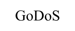
USPTO serial 99760695
GODOS
Reviewed by CopyMark Law Group
Status 653
- Filing date
- Status date
- Registration date
- —
- Examiner
- ROCCA, ALAINA M
- Law office
- TMEG LAW OFFICE 104
What this means
This page summarizes the public USPTO record for this serial number, including owners, goods and services, and prosecution history.
Need help with GODOS?
If you own this trademark, we can monitor new filings and help with USPTO deadlines. If you do not, we can file a new U.S. application.
Current trademark owner
Monitor this mark, or talk with CopyMark about this registration.
Not the owner?
File a new U.S. trademark application, or speak with our attorneys.
Owner
Attorney of record
The USPTO lists this attorney as the applicant's representative for correspondence on this application.
Michael T. Smith
Michael T. Smith Birch Stewart Kolasch & Birch, LLP2600 Park Tower Drive, Suite 600Vienna, VA 22180United StatesGoods and services
| Class | Description | Status | First use |
|---|---|---|---|
| 009 | Integrated circuit chips; Reticle, namely, optical detection apparatus for detecting ambient lights; Circuit boards provided with integrated circuits; Semi-conductors; Integrated circuit substrate, namely, silicon wafer, silicon carbide (SiC) and gallium nitride (GaN) wafers, germanium (Ge) wafer for use in fabrication of integrated circuits; Interface cards for data processing equipment in the form of printed circuits; Circuit boards; Silicon wafers; Integrated circuits; Electronic circuits; Printed circuit boards; Semiconductor chips; Semiconductor devices; Very large scale integration (VLSI) semiconductor integrated circuits; Circuit boards provided with integrated circuits; Semiconductor wafers; Wafers for integrated circuits; Motherboards; Large scale integrated circuits; Microchips; Electric or electronic sensors for detecting images; Piezoelectric sensors; Electric or electronic sensors for pressure; Optical sensor; Video phones | ACTIVE | — |
| 040 | Crystal wafer etching treatment; Semiconductor sealing processing; Integrated circuit etching treatment; Custom manufacturing of semi-conductors, chips and integrated circuits; Wafer Foundry, namely, custom manufacture of semiconductor wafers for others; Metal cutting treatment; Metal polishing treatment; Metal forging treatment; Metal tempering; Metal rust-resistant treatment; Metal plating; Cadmium plating; Chromium plating; Galvanization; Gold plating; Nickel plating; Silver plating; Tin plating; Electroplating; Laminating of metal plates and plastic sheets; Metal casting; Blacksmithing; Metal welding treatment; Welding services; Metal treating; Grinding; Burnishing by abrasion | ACTIVE | — |
Related trademarks
CopyMark links this record to cited §2(d) serials, the owner's other marks, Nice classes, similar mark names, and recently changed USPTO applications.
Prosecution history
| Date | Code | Event | What it means |
|---|---|---|---|
| Nov 3, 2026 | ERSI | TEAS RESPONSE TO SUSPENSION INQUIRY RECEIVED | — |
| Sep 23, 2026 | GNS3 | NOTIFICATION OF LETTER OF SUSPENSION E-MAILED | — |
| Sep 23, 2026 | GNSL | LETTER OF SUSPENSION E-MAILED | — |
| Sep 23, 2026 | CNSL | SUSPENSION LETTER WRITTEN | — |
| Sep 22, 2026 | TEME | TEAS/EMAIL CORRESPONDENCE ENTERED | — |
| Sep 22, 2026 | CRFA | CORRESPONDENCE RECEIVED IN LAW OFFICE | — |
| Sep 22, 2026 | TROA | TEAS RESPONSE TO OFFICE ACTION RECEIVED | This event means the applicant filed a response to a USPTO Office Action — typically arguments, amendments, or evidence addressing the examiner's objections. The USPTO will review the response and either allow the mark to proceed or issue another action. |
| Aug 28, 2026 | GNRN | NOTIFICATION OF NON-FINAL ACTION E-MAILED | A non-final Office Action means the USPTO examining attorney has raised at least one issue with your trademark application but has not made a final decision. You usually have three months to respond with arguments, amendments, or evidence. Missing the deadline can abandon the application. |
| Aug 28, 2026 | GNRT | NON-FINAL ACTION E-MAILED | A non-final Office Action means the USPTO examining attorney has raised at least one issue with your trademark application but has not made a final decision. You usually have three months to respond with arguments, amendments, or evidence. Missing the deadline can abandon the application. |
| Aug 28, 2026 | CNRT | NON-FINAL ACTION WRITTEN | A non-final Office Action means the USPTO examining attorney has raised at least one issue with your trademark application but has not made a final decision. You usually have three months to respond with arguments, amendments, or evidence. Missing the deadline can abandon the application. |
| Aug 20, 2026 | DOCK | ASSIGNED TO EXAMINER | — |
| Jul 30, 2026 | NWOS | NEW APPLICATION OFFICE SUPPLIED DATA ENTERED | — |
| Apr 13, 2026 | MAFR | APPLICATION FILING RECEIPT MAILED | — |
| Apr 13, 2026 | NWAP | NEW APPLICATION ENTERED | — |