
USPTO serial 99811360
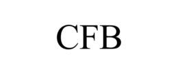
CFB
Reviewed by CopyMark Law Group
Status 641Office Action
- Filing date
- Status date
- Registration date
- —
- Examiner
- RENNEKER, CHRISTOPHER JOHN
- Law office
- TMO LAW OFFICE 113
What this means
The USPTO has issued an Office Action on this application. A response is typically required before the deadline, or the application can be abandoned.
Need help with CFB?
If you own this trademark, we can monitor new filings and help with USPTO deadlines. If you do not, we can file a new U.S. application.
Current trademark owner
Get help with this Office Action, set up monitoring, or talk with CopyMark.
Not the owner?
File a new U.S. trademark application, or speak with our attorneys.
Owner
Attorney of record
The USPTO lists this attorney as the applicant's representative for correspondence on this application.
Perla M. Kuhn
Perla M. Kuhn Gottlieb, Rackman & Reisman, P.C.270 Madison Avenue, Suite 1403New York, NY 10016United StatesGoods and services
| Class | Description | Status | First use |
|---|---|---|---|
| 009 | Semiconductor wafers; semiconductor substrates; semiconductor elements; light emitting diode chips; light emitting diode elements; photodiodes; integrated circuits; diode arrays; semiconductors; semiconductor devices formed by bonding heterogeneous materials; semiconductor devices; semiconductor wafers with thin films bonded together using epitaxial technology; optical semiconductors. | ACTIVE | — |
| 040 | Processing and manufacturing of semiconductor wafers; assembling and processing of semiconductor elements; manufacturing, assembling and processing services of semiconductor components and integrated circuits; assembling and packing for semiconductors and integrated circuits; assembling and packaging of semiconductor wafers and integrated circuits; custom manufacturing of wafer components (thin films using epitaxial technology), wafer IC chips, printed circuit boards, and semiconductor circuits; custom manufacturing of semiconductor wafers for others (including bonding thin films using epitaxial technology to semiconductor wafers); custom manufacturing and processing of thin semiconductor films on semiconductor substrates. | ACTIVE | — |
| 042 | (Class 42) Research in the field of semiconductor processing technology; testing, research and development relating to electronic circuits, semiconductor elements, integrated circuits and large scale integrated circuits; designing of electronic circuits, semiconductor elements, integrated circuits and large scale integrated circuits. | ACTIVE | — |
Related trademarks
CopyMark links this record to cited §2(d) serials, the owner's other marks, Nice classes, similar mark names, and recently changed USPTO applications.
Prosecution history
| Date | Code | Event | What it means |
|---|---|---|---|
| Sep 10, 2026 | GNRN | NOTIFICATION OF NON-FINAL ACTION E-MAILED | A non-final Office Action means the USPTO examining attorney has raised at least one issue with your trademark application but has not made a final decision. You usually have three months to respond with arguments, amendments, or evidence. Missing the deadline can abandon the application. |
| Sep 10, 2026 | GNRT | NON-FINAL ACTION E-MAILED | A non-final Office Action means the USPTO examining attorney has raised at least one issue with your trademark application but has not made a final decision. You usually have three months to respond with arguments, amendments, or evidence. Missing the deadline can abandon the application. |
| Sep 10, 2026 | CNRT | NON-FINAL ACTION WRITTEN | A non-final Office Action means the USPTO examining attorney has raised at least one issue with your trademark application but has not made a final decision. You usually have three months to respond with arguments, amendments, or evidence. Missing the deadline can abandon the application. |
| Sep 10, 2026 | DOCK | ASSIGNED TO EXAMINER | — |
| Jul 31, 2026 | NWOS | NEW APPLICATION OFFICE SUPPLIED DATA ENTERED | — |
| Jul 9, 2026 | TCCA | TEAS CHANGE OF CORRESPONDENCE RECEIVED | — |
| Jul 9, 2026 | ECDR | TEAS CHANGE OF DOMESTIC REPRESENTATIVES ADDRESS | — |
| Jul 9, 2026 | ARAA | ATTORNEY/DOM.REP.REVOKED AND/OR APPOINTED | This event means the applicant filed a response to a USPTO Office Action — typically arguments, amendments, or evidence addressing the examiner's objections. The USPTO will review the response and either allow the mark to proceed or issue another action. |
| Jul 9, 2026 | REAP | TEAS REVOKE/APP/CHANGE ADDR OF ATTY/DOM REP RECEIVED | — |
| Jul 9, 2026 | CHAN | APPLICANT/CORRESPONDENCE CHANGES (NON-RESPONSIVE) ENTERED | — |
| Jul 9, 2026 | COAR | TEAS CHANGE OF OWNER ADDRESS RECEIVED | — |
| May 8, 2026 | MAFR | APPLICATION FILING RECEIPT MAILED | — |
| May 8, 2026 | NWAP | NEW APPLICATION ENTERED | — |